
March 27, 2026
The Advanced Engineer's Guide to Custom PCB Design and Manufacturing
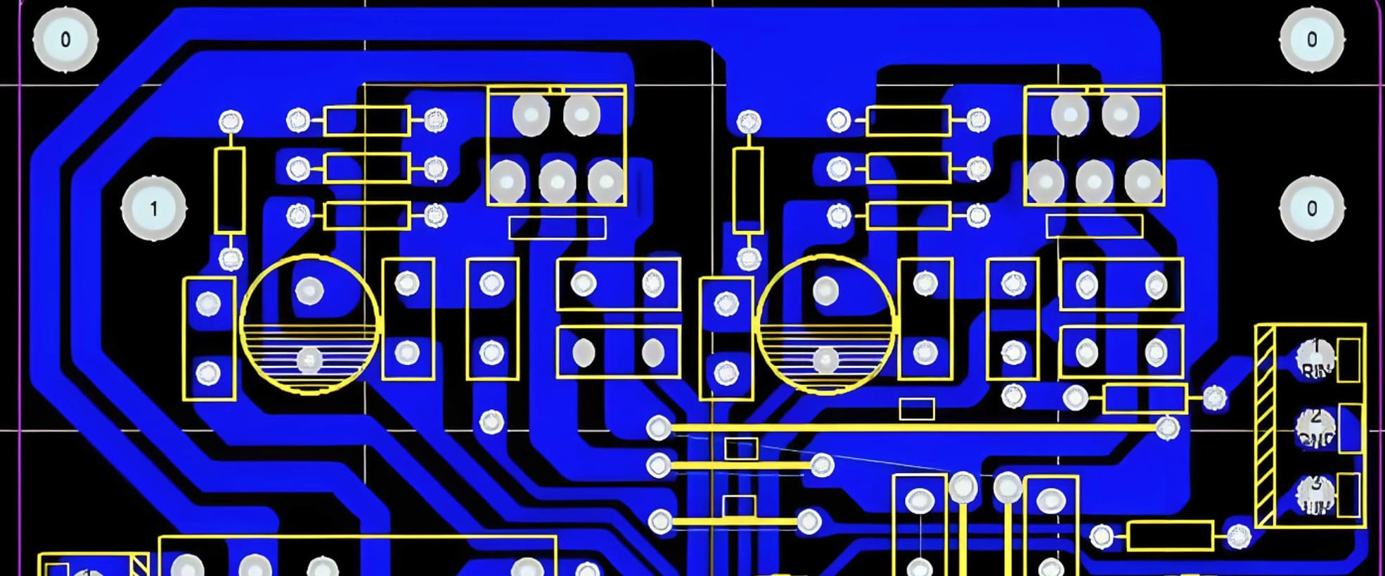
The Printed Circuit Board (PCB) serves as the physical and electrical foundation for all modern hardware. Whether engineering an industrial IoT gateway, a high-frequency aerospace communication module, or a high-density consumer device, mastering advanced multilayer PCB design guidelines dictates the reliability, signal integrity, and lifecycle of the hardware. Transitioning a conceptual schematic into a functional board requires more than just connecting nodes; it demands rigorous impedance planning, component library management, thermal dissipation strategies, and a deep understanding of Custom PCB Manufacturing Services.
Foundational Prep: Metadata and PCB Footprint Library Creation
Before attempting to layout a complex board, engineering teams must establish flawless component libraries. Industry failure analysis indicates that footprint-to-pad discrepancies account for approximately 40% of first-run prototype respins. A standard, error-free workflow relies heavily on meticulous PCB footprint library creation. This involves two synchronized elements:
- Schematic Symbols: Defining logical pinouts, linking Manufacturer Part Numbers (MPN), and embedding parametric metadata (tolerance, voltage rating, dielectric type) for automated Bill of Materials (BOM) generation.
- PCB Footprints: Containing the exact physical dimensions, courtyard outlines, and pad geometries. Strictly adhering to the IPC-7351 standard ensures optimal solder paste distribution and ideal fillet formation during automated assembly.
Advanced Substrate Selection: FR4 PCB Material Selection vs. High-Frequency Laminates
The choice of dielectric material fundamentally alters the board's electrical performance. While standard FR4 PCB material selection is sufficient for low-speed logic and basic power regulators, modern high-speed interfaces (such as PCIe Gen 4, DDR5, and RF antennas) demand strictly controlled impedance and low-loss tangents.
| Material Type | Dielectric Constant (Dk) | Dissipation Factor (Df) | Primary Application |
|---|---|---|---|
| Standard FR4 (Tg 130°C) | ~4.5 | 0.020 | General consumer electronics, microcontrollers, standard logic. |
| High-Tg FR4 (Tg 170°C+) | ~4.4 | 0.015 | Industrial controllers, automotive, high-layer-count HDI boards. |
| Rogers 4350B / Isola | 3.48 | 0.0037 | RF/Microwave communication, radar, 5G base stations. |
Signal Integrity and High-Speed PCB Routing Techniques
Component placement and trace routing dictate signal integrity. A fragmented layout forces convoluted routing, which degrades high-speed signals and amplifies Electromagnetic Interference (EMI). Utilizing high-speed PCB routing techniques is mandatory when clock speeds exceed 50MHz or rise times drop below 1 nanosecond.
Engineers must group components logically based on the schematic's netlist. Mastering controlled impedance PCB routing requires calculating exact trace widths and spacing using a 2D field solver, factoring in the copper weight, prepreg thickness, and the chosen core material.
| Routing Category | Engineering Guideline |
|---|---|
| Differential Pairs | Maintain continuous coupling (e.g., 90Ω for USB, 100Ω for Ethernet). Apply phase-matching meanders near the source of the mismatch, not the destination. |
| Cross-Talk Prevention | Implement the "3W Rule": The distance between the centers of adjacent high-speed traces must be at least three times the trace width. Route adjacent signal layers orthogonally. |
| Reference Planes | Never route high-frequency traces over a gap in the ground or power plane. This creates a slot antenna effect, radiating EMI and significantly increasing the return path loop inductance. |
Power Distribution Network (PDN) and Thermal Management
A robust Power Distribution Network (PDN) ensures stable, noise-free voltage delivery across the entire board under dynamic transient loads. High-current designs rely on dedicated power planes and large polygon copper pours rather than thin traces to minimize IR drop (voltage drop due to copper resistance).
Thermal management is intrinsically linked to the PDN. High-power components—like DFN-packaged MOSFETs, LDO linear regulators, and motor drivers—generate significant thermal density. Engineers must implement thermal via arrays (typically 0.3mm drill holes with 0.6mm pads) inside exposed ground pads to wick heat away from the surface into internal heavy-copper planes. Additionally, utilizing thermal relief spokes on standard through-hole components prevents "tombstoning" or cold solder joints by ensuring balanced heat dissipation during the reflow process.
Design for Manufacture (DFM) and the SMT Assembly Process Steps
The transition from a digital ECAD layout to a physical bare board requires stringent Design for Manufacturing (DFM) and Design for Assembly (DFA) verification. Submitting unverified Gerber, NC Drill files, or ODB++ packages to a fab house frequently triggers engineering holds, derailing project timelines.
Understanding the actual SMT assembly process steps allows designers to optimize their layouts for mass production. This includes integrating global and local fiducial markers (typically 1mm bare copper dots with a 3mm solder mask opening) which are absolutely mandatory for the optical alignment systems of automated Pick-and-Place machines.
| Fabrication Parameter | Standard IPC Class 2 Tolerance | Advanced HDI (High-Density Interconnect) |
|---|---|---|
| Trace Width / Spacing | 5 mil / 5 mil (0.127mm) | 3 mil / 3 mil (0.075mm) |
| Minimum Mechanical Drill | 0.20 mm - 0.30 mm | 0.10 mm (Laser drilled microvias) |
| Minimum Annular Ring | 6 mil (0.15mm) | 4 mil (0.10mm) |
| BGA Pitch Clearance | 0.80 mm | 0.40 mm - 0.30 mm (Requires via-in-pad) |
When dealing with mass production volumes, defining the correct panelization strategy—choosing between V-scoring for straight PCB edges or routing with mouse bites for curved, complex outlines—ensures structural integrity during SMT transport while allowing for clean de-panelization post-assembly. Partnering directly with a tier-one manufacturing facility to run strict DRC (Design Rule Checks) against their specific etching limits and copper tolerances before the final tape-out minimizes lead times, drives down unit costs, and maximizes the critical first-pass yield of the hardware launch.